2016年8月30日星期二
Samsung offers new ePoP memory for smartphones
High-end smartphones to come, if they could talk, would deliver a message to Samsung, relaying thanks for the memory. Samsung Electronics has announced they are mass-producing an "embedded package on package" (ePoP) memory for use in high-end smartphones. Samsung said this is a tech improvement over existing two-package eMCP memory solutions. This presents an opportunity for more space for a battery pack in slim handsets. In talking about the ePoP phone memory stack, Korea IT Times described ePOP as "a memory chip package that combines DRAM, NAND flash and controller into one memory, enabling them to be piled on top of a mobile application processor."
The Samsung announcement was posted on the Samsung Electronics official global blog. The announcement said that this is a memory package with 3GB LPDDR3 DRAM, 32GB embedded multimedia card and a controller. The saved-space factor is key to the news; ePoP combines all essential memory components into a single package which can be stacked directly on top of the mobile processor without taking up any additional space—all memory on a single ePoP module. Samsung said ePoP does not need any space beyond the 225 square millimeters (15x15mm) taken up by the mobile application processor. Samsung also said the 3GB LPDDR3 mobile DRAM inside the ePoP operates at an I/O data transfer rate of 1,866Mb/s, with a 64-bit I/O bandwidth.
The one-package memory solution was created to address market needs for high speed, high energy efficiency and compactness. Jeeho Baek, senior vice president of memory marketing at Samsung Electronics, said Samsung expects to provide customers with "significant design benefits" along with faster, longer operations of multi-tasking features. Phone manufacturers can use the available space for components such as the battery pack. The new memory solution could save up to 40 percent of space in a smartphone.
The phone has special heat-resistant properties; Business Korea said, "As NAND flash is generally sensitive to heat, it was previously thought to be difficult to stack any above a mobile AP that processes at a high temperature. However, Samsung Electronics raised the heat resistance limit of its NAND flash, breaking the common idea in the industry, and launched ePoP, calling it 'wearable memory.'" Samsung has already been offering a similar single-package solution for wearable devices; the new configuration can be customized for flagship smartphones.
Going further into translation of how this might affect consumer phones, BGR's Chris Smith said on Thursday that people looking forward to seeing some of Samsung's 2015 "top-shelf devices in stores, including the Galaxy S6," might have reason to be excited about this new type of component. Since more space is cleared inside a mobile device, there is the opportunity of expanding the battery capacity of the device. "That's particularly useful for slimmer smartphones," said Smith, "as smartphone makers have yet to crack the battery problem and are still trying to figure out ways of improving smartphone battery life."
Will ePoP chips be a factor in Galaxy S6 phones? Even if not, Smith said that "such ePoP designs could be used in upcoming flagship smartphones and tablets, even if the Galaxy S6 is skipped."
2016年8月29日星期一
New hacking technique imperceptibly changes memory virtual servers
Using a new attack technique, a team of Dutch hacking experts managed to alter the memory of virtual machines in the cloud without a software bug.
With this technique an attacker can crack the keys of secured virtual machines or install malware without being noticed. It's a new deduplication-based attack in which data can not only be viewed and leaked, but also modified using a hardware glitch. By doing so the attacker can order the server to install malicious and unwanted software or allow logins by unauthorized persons.
Deduplication and Rowhammer bug
With the new attack technique Flip Feng Shui (FSS), an attacker rents a virtual machine on the same host as the victim. This can be done by renting many virtual machines until one of them lands next to the victim. A virtual machine in the cloud is often used to run applications, test new software, or run a website. There are public (for everyone), community (for a select group) and private (for one organization accessible) clouds. The attacker writes a memory page that he knows exists in the victim on the vulnerable memory location and lets it deduplicate. As a result, the identical pages will be merged into one in order to save space (the information is, after all, the same). That page is stored in the same part of the memory of the physical computer. The attacker can now modify the information in the general memory of the computer. This can be done by triggering a hardware bug dubbed Rowhammer, which causes flip bits from 0 to 1 or vice versa, to seek out the vulnerable memory cells and change them.
Cracking OpenSSH
The researchers of the Vrije Universiteit Amsterdam, who worked together with a researcher from the Catholic University of Leuven, describe in their research two attacks on the operating systems Debian and Ubuntu. The first FFS attack gained access to the virtual machines through weakening OpenSSH public keys. The attacker did this by changing the victim's public key with one bit. In the second attack, the settings of the software management application apt were adjusted by making minor changes to the URL from where apt downloads software. The server could then install malware that presents itself as a software update. The integrity check could be circumvented by making a small change to the public key that verifies the integrity of the apt-get software packages.
Advise NSCS
Debian, Ubuntu, OpenSSH and other companies included in the research were notified before the publication and all have responded. The National Cyber Security Centre (NSCS) of the Dutch government has issued a fact sheet containing information and advice on FFS.
'Hack-Oscar'
The researchers presented their findings this week during the UNESIX Security Symposium 2016 in the United States. Recently they won the Oscar of hacking: the Pwnie for another attack technique that allows attackers to take over state-of-the-art software with all defences up, even if the software has no bugs.
2016年8月28日星期日
New thin film transistor may open the door to the development of flexible electronic devices
The thin electronic devices could open the door to the development of flexible electronic devices with applications as wide-ranging as display technology to medical imaging and renewable energy production.
The team was exploring new uses for thin film transistors (TFT), which are most commonly found in low-power, low-frequency devices like the display screen you're reading from now. Efforts by researchers and the consumer electronics industry to improve the performance of the transistors have been slowed by the challenges of developing new materials or slowly improving existing ones for use in traditional thin film transistor architecture, known technically as the metal oxide semiconductor field effect transistor (MOSFET).
But the U of A electrical engineering team did a run-around on the problem. Instead of developing new materials, the researchers improved performance by designing a new transistor architecture that takes advantage of a bipolar action. In other words, instead of using one type of charge carrier, as most thin film transistors do, it uses electrons and the absence of electrons (referred to as "holes") to contribute to electrical output. Their first breakthrough was forming an 'inversion' hole layer in a 'wide-bandgap' semiconductor, which has been a great challenge in the solid-state electronics field.
Once this was achieved, "we were able to construct a unique combination of semiconductor and insulating layers that allowed us to inject "holes" at the MOS interface," said Gem Shoute, a PhD student in the Department of Electrical and Computer Engineering who is lead author on the article. Adding holes at the interface increased the chances of an electron "tunneling" across a dielectric barrier. Through this phenomenon, a type of quantum tunnelling, "we were finally able to achieve a transistor that behaves like a bipolar transistor."
"It's actually the best performing [TFT] device of its kind—ever," said materials engineering professor Ken Cadien, a co-author on the paper. "This kind of device is normally limited by the non-crystalline nature of the material that they are made of"
The dimension of the device itself can be scaled with ease in order to improve performance and keep up with the need of miniaturization, an advantage that modern TFTs lack. The transistor has power-handling capabilities at least 10 times greater than commercially produced thin film transistors.
Electrical engineering professor Doug Barlage, who is Shoute's PhD supervisor and one of the paper's lead authors, says his group was determined to try new approaches and break new ground. He says the team knew it could produce a high-power thin film transistor—it was just a matter of finding out how.
"Our goal was to make a thin film transistor with the highest power handling and switching speed possible. Not many people want to look into that, but the raw properties of the film indicated dramatic performance increase was within reach," he said. "The high quality sub 30 nanometre (a human hair is 50 micrometres wide) layers of materials produced by Professor Cadien's group enabled us to successfully try these difficult concepts"
In the end, the team took advantage of the very phenomena other researchers considered roadblocks.
"Usually tunnelling current is considered a bad thing in MOSFETs and it contributes to unnecessary loss of power, which manifests as heat," explained Shoute. "What we've done is build a transistor that considers tunnelling current a benefit."
The team has filed a provisional patent on the transistor. Shoute says the next step is to put the transistor to work "in a fully flexible medium and apply these devices to areas like biomedical imaging, or renewable energy."
2016年8月26日星期五
There is a possibility that Smart chip makes low-powered, wireless neural implants
A small smart chip has been developed by Scientists at Nanyang Technological University, Singapore (NTU Singapore) that can be paired with neural implants for efficient wireless transmission of brain signals.
"It is about a hundred times more efficient than current processing chips on the market. It will lead to more compact medical wearable devices, such as portable ECG monitoring devices and neural implants, since we no longer need large batteries to power them."
Neural implants when embedded in the brain can alleviate the debilitating symptoms of Parkinson's disease or give paraplegic people the ability to move their prosthetic limbs.
However, they need to be connected by wires to an external device outside the body. For a prosthetic patient, the neural implant is connected to a computer that decodes the brain signals so the artificial limb can move.
These external wires are not only cumbersome but the permanent openings which allow the wires into the brain increases the risk of infections.
The new chip by NTU scientists can allow the transmission of brain data wirelessly and with high accuracy.
Assistant Professor Arindam Basu from NTU's School of Electrical and Electronic Engineering said the research team have tested the chip on data recorded from animal models, which showed that it could decode the brain's signal to the hand and fingers with 95 per cent accuracy.
"What we have developed is a very versatile smart chip that can process data, analyse patterns and spot the difference," explained Prof Basu.
Different from other wireless implants
To achieve high accuracy in decoding brain signals, implants require thousands of channels of raw data. To wirelessly transmit this large amount of data, more power is also needed which means either bigger batteries or more frequent recharging.
This is not feasible as there is limited space in the brain for implants while frequent recharging means the implants cannot be used for long-term recording of signals.
Current wireless implant prototypes thus suffer from a lack of accuracy as they lack the bandwidth to send out thousands of channels of raw data.
Instead of enlarging the power source to support the transmission of raw data, Asst Prof Basu tried to reduce the amount of data that needs to be transmitted.
Designed to be extremely power-efficient, NTU's patented smart chip will analyse and decode the thousands of signals from the neural implants in the brain, before compressing the results and sending it wirelessly to a small external receiver.
This invention and its findings were published last month in the prestigious journal, IEEE Transactions on Biomedical Circuits & Systems, by the Institute of Electrical and Electronics Engineers, the world's largest professional association for the advancement of technology.
Its underlying science was also featured in three international engineering conferences (two in Atlanta, USA and one in China) over the last three months.
Versatile smart chip with multiple uses
This new smart chip is designed to analyse data patterns and spot any abnormal or unusual patterns.
For example, in a remote video camera, the chip can be programmed to send a video back to the servers only when a specific type of car or something out of the ordinary is detected, such as an intruder.
This would be extremely beneficial for the Internet of Things (IOT), where every electrical and electronic device is connected to the Internet through a smart chip.
With a report by marketing research firm Gartner Inc predicting that 6.4 billion smart devices and appliances will be connected to the Internet by 2016, and will rise to 20.8 billion devices by 2020, reducing network traffic will be a priority for most companies.
Using NTU's new chip, the devices can process and analyse the data on site, before sending back important details in a compressed package, instead of sending the whole data stream. This will reduce data usage by over a thousand times.
Asst Prof Basu is now in talks with Singapore Technologies Electronics Limited to adapt his smart chip that can significantly reduce power consumption and the amount of data transmitted by battery-operated specialized sensors, such as video cameras.
The team is also looking to expand the applications of the chip into commercial products, such as to customise it for smart home sensor networks, in collaboration with a local electronics company.
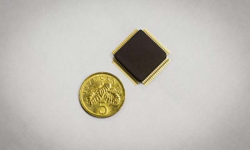
The chip, measuring 5mm by 5mm can now be licensed by companies from NTU's commercialisation arm, NTUitive.
2016年8月25日星期四
Samsung brings in world's first universal flash storage removable memory card line-up
"Our new 256GB UFS card will provide an ideal user experience for digitally-minded consumers and lead the industry in establishing the most competitive memory card solution," said Jung-bae Lee, senior vice president, Memory Product Planning & Application Engineering, Samsung Electronics "By launching our new high-capacity, high-performance UFS card line-up, we are changing the growth paradigm of the memory card market to prioritize performance and user convenience above all."
Samsung's new 256GB UFS removable memory card ─ simply referred to as the UFS card will provide greatly improved user experiences, especially in high-resolution 3D gaming and high-resolution movie playback. It provides more than five times faster sequential read performance compared to that of a typical microSD card, reading sequentially at 530 megabytes per second (MB/s) which is similar to the sequential read speed of the most widely used SATA SSDs. With this UFS card, consumers have the ability to read a 5GB, Full-HD movie in approximately 10 seconds, compared to a typical UHS-1 microSD card, which would take over 50 seconds with 95MB/s of sequential reading speed. Also, at a random read rate of 40,000 IOPS, the 256GB card delivers more than 20 times higher random read performance compared to a typical microSD, which offers approximately 1,800 IOPS.
When it comes to writing, the new 256GB UFS card processes 35,000 random IOPS, which is 350 times higher than the 100 IOPs of a typical microSD card, and attains a 170MB/s sequential write speed, almost doubling the top-end microSD card speed. With these substantial performance improvements, the new 256GB UFS card significantly reduces multimedia data downloading time, photo thumbnail loading time and buffer clearing time in burst shooting mode, which, collectively, can be particularly beneficial to DSLR camera users. To shoot 24 large/extra fine JPEG photographs (1,120 megabyte (MB)-equivalent) continuously with a high-end DSLR camera, the 256GB UFS card takes less than seven seconds, compared to a UHS-1 microSD card which typically takes about 32 seconds, at 35MB/s.
To achieve the highest performance and most power-efficient data transport, the UFS card supports multiple commands with command queuing features and enables simultaneous reading and writing through the use of separately dedicated paths, doubling throughput.
Samsung has been aggressive in preparing UFS solutions for the marketplace, while contributing to JEDEC standardization of the Universal Flash Storage 2.0 specification in September 2013 and the Universal Flash Storage (UFS) 1.0 Card Extension standard in March 2016. Following its introduction of the industry-first 128GB embedded UFS chip in January 2015, the company successfully launched a 256GB embedded UFS memory for high-end mobile devices in February of this year. As of earlier this month, Samsung also completed the Universal Flash Storage Association (UFSA)'s certification program that evaluates electrical and functional specifications for compatibility of a UFS card, and Samsung's new UFS card products were approved as UFSA-certified UFS cards with the right to use the official UFS logo for the first time in the industry.
2016年8月24日星期三
A rechargeable battery to power a home from rooftop solar panels
Scientists have said that a rechargeable battery that could make storage of electricity from intermittent energy sources like solar and wind safe and cost-effective for both residential and commercial use. The new research builds on earlier work by members of the same team that could enable cheaper and more reliable electricity storage at the grid level.
The mismatch between the availability of intermittent wind or sunshine and the variability of demand is a great obstacle to getting a large fraction of our electricity from renewable sources. This problem could be solved by a cost-effective means of storing large amounts of electrical energy for delivery over the long periods when the wind isn't blowing and the sun isn't shining.
In the operation of the battery, electrons are picked up and released by compounds composed of inexpensive, earth-abundant elements (carbon, oxygen, nitrogen, hydrogen, iron and potassium) dissolved in water. The compounds are non-toxic, non-flammable, and widely available, making them safer and cheaper than other battery systems.
"This is chemistry I'd be happy to put in my basement," says Michael J. Aziz, Gene and Tracy Sykes Professor of Materials and Energy Technologies at Harvard Paulson School of Engineering and Applied Sciences (SEAS), and project Principal Investigator. "The non-toxicity and cheap, abundant materials placed in water solution mean that it's safe—it can't catch on fire—and that's huge when you're storing large amounts of electrical energy anywhere near people."
This new rechargeable battery chemistry was discovered by post-doctoral fellow Michael Marshak and graduate student Kaixiang Lin working together with co-lead author Roy Gordon, Thomas Dudley Cabot Professor of Chemistry and Professor of Materials Science at Harvard.
"We combined a common organic dye with an inexpensive food additive to increase our battery voltage by about 50 percent over our previous materials," says Gordon. The findings "deliver the first high-performance, non-flammable, non-toxic, non-corrosive, and low-cost chemicals for flow batteries."
Unlike solid-electrode batteries, flow batteries store energy in liquids contained in external tanks, similar to fuel cells. The tanks (which set the energy capacity), as well as the electrochemical conversion hardware through which the fluids are pumped (which sets peak power capacity), can be sized independently. Since the amount of energy that can be stored can be arbitrarily increased by scaling up only the size of the tanks, larger amounts of energy can be stored at lower cost than traditional battery systems.
The active components of electrolytes in most flow battery designs have been metal ions such as vanadium dissolved in acid. The metals can be expensive, corrosive, tricky to handle, and kinetically sluggish, leading to inefficiencies. Last year, Aziz and his Harvard colleagues demonstrated a flow battery that replaced metals with organic (carbon-based) molecules called quinones, which are abundant, naturally occurring chemicals that are integral to biological processes like photosynthesis and cellular respiration. While quinones in aqueous solution formed the negative electrolyte side of the battery, the positive side relied on a conventional bromine-bearing electrolyte that is used in several other batteries. The high performance and low cost of the technology, which Harvard has licensed to a company in Europe, hold the potential to provide scalable grid-level storage solutions to utilities.
But bromine's toxicity and volatility make it most suitable for settings where trained professionals can deal with it safely behind secure fences.
So the team began searching for a new recipe that would provide comparable storage advantages—inexpensive, long lasting, efficient—using chemicals that could be safely deployed in homes and businesses. Their new battery, described in a paper published today in the journal Science, replaces bromine with a non-toxic and non-corrosive ion called ferrocyanide.
"It sounds bad because it has the word 'cyanide' in it," explains co-lead author Marshak, who is now assistant professor of chemistry at the University of Colorado Boulder. "Cyanide kills you because it binds very tightly to iron in your body. In ferrocyanide, it's already bound to iron, so it's safe. In fact, ferrocyanide is commonly used as a food additive, and also as a fertilizer."
Because ferrocyanide is highly soluble and stable in alkaline rather than acidic solutions, the Harvard team paired it with a quinone compound that is soluble and stable under alkaline conditions, in contrast to the acidic environment of their original battery developed last year.
Marshak compares exposure to the concentrated alkaline solution to coming into contact with a damaged disposable AA battery. "It's not something you want to eat or splash around in, but outside of that it's really not a problem."
There are other advantages to using alkaline solution. Because it is non-corrosive, the flow battery system components can be constructed of simpler and much less expensive materials such as plastics.
"First generation flow batteries were single-element couples - transition metals like vanadium or iron or chrome," says Michael Perry, Project Leader for Electrochemical Systems at United Technologies Research Center, who was not involved in the work. "Now we're seeing the possibility of engineered molecules giving us the properties and attributes that we want in one complete system. More work is required and justified but the Harvard team is really demonstrating the promise of next-generation chemistries."
Robert F. Savinell, Distinguished University Professor and George S. Dively Professor of Engineering at Case Western Reserve University, another battery expert who was not part of the Harvard research, agrees that the new technology offers significant advantages over other flow batteries concepts, including "potential very low costs with sustainable materials, high efficiencies at practical power densities, and safe and simple operation." He adds: "It should be expected that this flow battery approach will have a short development and scale-up path for fast commercial introduction."
Harvard's Office of Technology Development has been working closely with the research team to navigate the shifting complexities of the energy storage market and build relationships with companies well positioned to commercialize the new chemistries.
The demand for battery storage is driven by regulatory factors as much as economic ones. In some states, as well as many parts of the world, if it can't be instantaneously used by meeting electricity demand, solar energy incident on solar panels goes to waste unless the electricity is stored. However, in many states, customers have the right to sell electricity produced by rooftop solar panels at high consumer rates under a regulatory scheme called net metering. Under those circumstances, consumers have little incentive to install batteries. But market experts like William W. Hogan, Raymond Plank Professor of Global Energy Policy at Harvard Kennedy School, believe that such policies are ultimately "uneconomic and unsustainable." And as more and more homeowners install solar panels, utilities are opposing requirements to buy electricity from their customers.
Hogan says net metering is one of a series of "regulatory gimmicks designed to make solar more attractive" and predicts that eventually consumers with rooftop photovoltaic panels will lose the option of exchanging electricity for discounts on their utility bills. When that happens, these homeowners have an incentive to invest in battery storage.
That's the emerging market opportunity that Tesla Motors entrepreneur Elon Musk hopes to leverage with his company's recently-announced Powerwall system. But the flow battery design engineered by Aziz and his Harvard colleagues offers potential advantages in cost and the length of time it can maintain peak discharge power compared to lithium batteries.
"This has potential because photovoltaics are growing so fast," Aziz says. "A cloud comes over your solar installation and BAM - the production goes crashing down. Then the cloud goes away and the production goes shooting up. The best way of dealing with that is with batteries."
2016年8月22日星期一
A low-power always-on camera with gesture recognition has been developed recently
Smart devices that wake up with voice commands have gained popularity in recent years, and now researchers at Georgia Institute of Technology have taken it one step farther: an always-on camera.
Designed with a combination of low-power hardware and energy efficient image processing software, the always-on camera is capable of watching for specific types of movement without draining batteries or running up electricity bills.
"Right now cameras are very hard to run on passive power just because they burn so much power themselves," said Justin Romberg, a professor in Georgia Tech's School of Electrical and Computer Engineering. "This combination of efficient signal processing and a novel hardware design lowers the power requirement and means that some of these other options to power it might be open."
The research, which was highlighted at the International Symposium on Low Power Electronics and Design Aug. 8-10, was sponsored by Intel Corp. and the National Science Foundation.
While reducing the frame rate of a camera plays a role in lowering power demands, to achieve the power savings needed for this project, the researchers programmed the camera to track motion in a more generalized way that still preserved crucial details about what was being tracked. That requires much less power to process than tracking individual pixels throughout the entire field of view.
"What this camera is actually looking at is not pixel values, but pixels added together in all different ways and a dramatically smaller number of measurements than if you had it in a standard mode," Romberg said.
The always-on camera was primarily designed as a way to wake up devices. But its ability to recognize specific gestures expands the possibilities – such as a camera that wakes up with a specific pattern or movement almost like a secret handshake.
"We wanted to devise a camera that was capturing images all of the time, and then once you have a particular gesture – like you write a Z in the air – it's going to wake up," said Arijit Raychowdhury, an associate professor in the School of Electrical and Computer Engineering. "To make that work without affecting the battery life, we wanted it to be so low power that you can power it with harvested ambient energy, such as with a photovoltaic cell."
Programming a camera to recognize specific gestures and wake up only when needed is also a way of conserving total system energy, Raychowdhury said.
"Simple motion detection is a well-studied area of research, and there are commercial products that support motion detection," he said. "But the problem is that a camera that can just detect motion – and not specific patterns in motion or gestures – is going to wake up more often, even when it doesn't need to."
Such a low-power camera could be useful in a range of applications, especially for camera systems in remote locations where efficiency is crucial.
"If you have a camera in the field, you want them to use as little energy as possible and only record events when necessary," Romberg said.
Other applications include specialized surveillance, robotics and consumer electronics with hands-free operation, and the researchers are already working on adding wireless functionality to transmit images and data with an antenna.
订阅:
博文 (Atom)