2016年8月31日星期三

Tomorrow's clothes may be made with light-emitting e-fabric

September 1, 2016 by Lisa Zyga

Researchers have fabricated a large-area textile that emits bright yellow light for more than 180 hours. The low-cost, flexible, transparent textile has potential applications in light-emitting clothing, signs, and architectural features.
The scientists have published a paper on the light-emitting textile in a recent issue of Flexible and Printed Electronics.
"Our work shows that ultra-flexible light emission on large areas can be realized on very lightweight textile electrodes," coauthor Thomas Lanz at Umeå University told Phys.org. "Traditionally, this was hard to come by, as these electrodes are typically quite rough. We have demonstrated that the light-emitting electrochemical cell's inherent fault tolerance is ideally suited for this type of transparent substrate. We see great potential for this technology in the field of wearables, as the device is highly conformal."
As the researchers explain, the key advantages of the new fabric are its high flexibility, light weight, and low cost. Currently, the most common transparent and flexible light-emitting device technology is the organic light-emitting diode (OLED), whose fabrication process involves expensive vacuum technology. In addition, the transparent electrodes in many OLEDs are made of indium-tin oxide (ITO), a relatively scarce material that is expensive to use on a large scale.

In contrast, the light-emitting textile presented in the new study is realized by spray-coating a light-emitting electrochemical cell (LEC) onto a transparent fabric-based electrode, resulting in a simpler and less expensive fabrication process compared to that used to make OLEDs. The fabric electrode consists of a weave of silver-coated copper wires and polymer fibers that are embedded in a polymer matrix, all of which is coated with a conductive ink.
Tests showed that the new textile emits highly uniform, bright yellow light for more than 180 hours, with the efficiency and luminescence both increasing over time. The researchers attribute these characteristics to the dynamic doping process that renders the LEC highly fault-tolerant.
In the future, the researchers plan to scale up the device to cover even larger emission areas and to make it semi-transparent, both of which look promising due to the flexible fabrication process.

2016年8月30日星期二

Samsung offers new ePoP memory for smartphones


High-end smartphones to come, if they could talk, would deliver a message to Samsung, relaying thanks for the memory. Samsung Electronics has announced they are mass-producing an "embedded package on package" (ePoP) memory for use in high-end smartphones. Samsung said this is a tech improvement over existing two-package eMCP memory solutions. This presents an opportunity for more space for a battery pack in slim handsets. In talking about the ePoP phone memory stack, Korea IT Times described ePOP as "a memory chip package that combines DRAM, NAND flash and controller into one memory, enabling them to be piled on top of a mobile application processor."

The Samsung announcement was posted on the Samsung Electronics official global blog. The announcement said that this is a memory package with 3GB LPDDR3 DRAM, 32GB embedded multimedia card and a controller. The saved-space factor is key to the news; ePoP combines all essential memory components into a single package which can be stacked directly on top of the mobile processor without taking up any additional space—all memory on a single ePoP module. Samsung said ePoP does not need any space beyond the 225 square millimeters (15x15mm) taken up by the mobile application processor. Samsung also said the 3GB LPDDR3 mobile DRAM inside the ePoP operates at an I/O data transfer rate of 1,866Mb/s, with a 64-bit I/O bandwidth.

The one-package memory solution was created to address market needs for high speed, high energy efficiency and compactness. Jeeho Baek, senior vice president of memory marketing at Samsung Electronics, said Samsung expects to provide customers with "significant design benefits" along with faster, longer operations of multi-tasking features. Phone manufacturers can use the available space for components such as the battery pack. The new memory solution could save up to 40 percent of space in a smartphone.

The phone has special heat-resistant properties; Business Korea said, "As NAND flash is generally sensitive to heat, it was previously thought to be difficult to stack any above a mobile AP that processes at a high temperature. However, Samsung Electronics raised the heat resistance limit of its NAND flash, breaking the common idea in the industry, and launched ePoP, calling it 'wearable memory.'" Samsung has already been offering a similar single-package solution for wearable devices; the new configuration can be customized for flagship smartphones.

Going further into translation of how this might affect consumer phones, BGR's Chris Smith said on Thursday that people looking forward to seeing some of Samsung's 2015 "top-shelf devices in stores, including the Galaxy S6," might have reason to be excited about this new type of component. Since more space is cleared inside a mobile device, there is the opportunity of expanding the battery capacity of the device. "That's particularly useful for slimmer smartphones," said Smith, "as smartphone makers have yet to crack the battery problem and are still trying to figure out ways of improving smartphone battery life."

Will ePoP chips be a factor in Galaxy S6 phones? Even if not, Smith said that "such ePoP designs could be used in upcoming flagship smartphones and tablets, even if the Galaxy S6 is skipped."

2016年8月29日星期一

New hacking technique imperceptibly changes memory virtual servers


Using a new attack technique, a team of Dutch hacking experts managed to alter the memory of virtual machines in the cloud without a software bug.

With this technique an attacker can crack the keys of secured virtual machines or install malware without being noticed. It's a new deduplication-based attack in which data can not only be viewed and leaked, but also modified using a hardware glitch. By doing so the attacker can order the server to install malicious and unwanted software or allow logins by unauthorized persons.

Deduplication and Rowhammer bug
With the new attack technique Flip Feng Shui (FSS), an attacker rents a virtual machine on the same host as the victim. This can be done by renting many virtual machines until one of them lands next to the victim. A virtual machine in the cloud is often used to run applications, test new software, or run a website. There are public (for everyone), community (for a select group) and private (for one organization accessible) clouds. The attacker writes a memory page that he knows exists in the victim on the vulnerable memory location and lets it deduplicate. As a result, the identical pages will be merged into one in order to save space (the information is, after all, the same). That page is stored in the same part of the memory of the physical computer. The attacker can now modify the information in the general memory of the computer. This can be done by triggering a hardware bug dubbed Rowhammer, which causes flip bits from 0 to 1 or vice versa, to seek out the vulnerable memory cells and change them.

Cracking OpenSSH
The researchers of the Vrije Universiteit Amsterdam, who worked together with a researcher from the Catholic University of Leuven, describe in their research two attacks on the operating systems Debian and Ubuntu. The first FFS attack gained access to the virtual machines through weakening OpenSSH public keys. The attacker did this by changing the victim's public key with one bit. In the second attack, the settings of the software management application apt were adjusted by making minor changes to the URL from where apt downloads software. The server could then install malware that presents itself as a software update. The integrity check could be circumvented by making a small change to the public key that verifies the integrity of the apt-get software packages.

Advise NSCS
Debian, Ubuntu, OpenSSH and other companies included in the research were notified before the publication and all have responded. The National Cyber Security Centre (NSCS) of the Dutch government has issued a fact sheet containing information and advice on FFS.

'Hack-Oscar'
The researchers presented their findings this week during the UNESIX Security Symposium 2016 in the United States. Recently they won the Oscar of hacking: the Pwnie for another attack technique that allows attackers to take over state-of-the-art software with all defences up, even if the software has no bugs.

2016年8月28日星期日

New thin film transistor may open the door to the development of flexible electronic devices


The thin electronic devices could open the door to the development of flexible electronic devices with applications as wide-ranging as display technology to medical imaging and renewable energy production.
The team was exploring new uses for thin film  (TFT), which are most commonly found in low-power, low-frequency devices like the display screen you're reading from now. Efforts by researchers and the consumer electronics industry to improve the performance of the transistors have been slowed by the challenges of developing new materials or slowly improving existing ones for use in traditional thin film transistor architecture, known technically as the metal oxide semiconductor field effect transistor (MOSFET).
But the U of A electrical engineering team did a run-around on the problem. Instead of developing , the researchers improved performance by designing a new transistor architecture that takes advantage of a bipolar action. In other words, instead of using one type of charge carrier, as most thin film transistors do, it uses electrons and the absence of electrons (referred to as "holes") to contribute to electrical output. Their first breakthrough was forming an 'inversion' hole layer in a 'wide-bandgap' semiconductor, which has been a great challenge in the solid-state electronics field.
Once this was achieved, "we were able to construct a unique combination of semiconductor and insulating layers that allowed us to inject "holes" at the MOS interface," said Gem Shoute, a PhD student in the Department of Electrical and Computer Engineering who is lead author on the article. Adding holes at the interface increased the chances of an electron "tunneling" across a dielectric barrier. Through this phenomenon, a type of quantum tunnelling, "we were finally able to achieve a transistor that behaves like a bipolar transistor."
"It's actually the best performing [TFT] device of its kind—ever," said materials engineering professor Ken Cadien, a co-author on the paper. "This kind of device is normally limited by the non-crystalline nature of the material that they are made of"
The dimension of the device itself can be scaled with ease in order to improve performance and keep up with the need of miniaturization, an advantage that modern TFTs lack. The transistor has power-handling capabilities at least 10 times greater than commercially produced thin film transistors.
Electrical engineering professor Doug Barlage, who is Shoute's PhD supervisor and one of the paper's lead authors, says his group was determined to try new approaches and break new ground. He says the team knew it could produce a high-power thin film transistor—it was just a matter of finding out how.
"Our goal was to make a thin film transistor with the highest power handling and switching speed possible. Not many people want to look into that, but the raw properties of the film indicated dramatic performance increase was within reach," he said. "The high quality sub 30 nanometre (a human hair is 50 micrometres wide) layers of materials produced by Professor Cadien's group enabled us to successfully try these difficult concepts"
In the end, the team took advantage of the very phenomena other researchers considered roadblocks.
"Usually tunnelling current is considered a bad thing in MOSFETs and it contributes to unnecessary loss of power, which manifests as heat," explained Shoute. "What we've done is build a transistor that considers tunnelling current a benefit."
The team has filed a provisional patent on the transistor. Shoute says the next step is to put the transistor to work "in a fully flexible medium and apply these devices to areas like biomedical imaging, or renewable energy."

2016年8月26日星期五

There is a possibility that Smart chip makes low-powered, wireless neural implants

A small smart chip has been developed by Scientists at Nanyang Technological University, Singapore (NTU Singapore) that can be paired with neural implants for efficient wireless transmission of brain signals.

Neural implants when embedded in the brain can alleviate the debilitating symptoms of Parkinson's disease or give paraplegic people the ability to move their prosthetic limbs.
However, they need to be connected by wires to an external device outside the body. For a prosthetic patient, the neural implant is connected to a computer that decodes the brain signals so the artificial limb can move.
These external wires are not only cumbersome but the permanent openings which allow the wires into the brain increases the risk of infections.
The new chip by NTU scientists can allow the transmission of brain data wirelessly and with .
Assistant Professor Arindam Basu from NTU's School of Electrical and Electronic Engineering said the research team have tested the chip on data recorded from animal models, which showed that it could decode the brain's signal to the hand and fingers with 95 per cent accuracy.
"What we have developed is a very versatile smart chip that can process data, analyse patterns and spot the difference," explained Prof Basu.

"It is about a hundred times more efficient than current processing chips on the market. It will lead to more compact medical wearable devices, such as portable ECG monitoring devices and , since we no longer need large batteries to power them."


Different from other wireless implants
To achieve high accuracy in decoding , implants require thousands of channels of raw data. To wirelessly transmit this large amount of data, more power is also needed which means either bigger batteries or more frequent recharging.
This is not feasible as there is limited space in the brain for implants while frequent recharging means the implants cannot be used for long-term recording of signals.
Current wireless implant prototypes thus suffer from a lack of accuracy as they lack the bandwidth to send out thousands of channels of raw data.
Instead of enlarging the power source to support the transmission of raw data, Asst Prof Basu tried to reduce the amount of data that needs to be transmitted.
Designed to be extremely power-efficient, NTU's patented smart chip will analyse and decode the thousands of signals from the neural implants in the brain, before compressing the results and sending it wirelessly to a small external receiver.
This invention and its findings were published last month in the prestigious journal, IEEE Transactions on Biomedical Circuits & Systems, by the Institute of Electrical and Electronics Engineers, the world's largest professional association for the advancement of technology.
Its underlying science was also featured in three international engineering conferences (two in Atlanta, USA and one in China) over the last three months.
Versatile smart chip with multiple uses
This new smart chip is designed to analyse data patterns and spot any abnormal or unusual patterns.
For example, in a remote video camera, the chip can be programmed to send a video back to the servers only when a specific type of car or something out of the ordinary is detected, such as an intruder.
This would be extremely beneficial for the Internet of Things (IOT), where every electrical and electronic device is connected to the Internet through a smart chip.
With a report by marketing research firm Gartner Inc predicting that 6.4 billion smart devices and appliances will be connected to the Internet by 2016, and will rise to 20.8 billion devices by 2020, reducing network traffic will be a priority for most companies.
Using NTU's new chip, the devices can process and analyse the data on site, before sending back important details in a compressed package, instead of sending the whole data stream. This will reduce data usage by over a thousand times.
Asst Prof Basu is now in talks with Singapore Technologies Electronics Limited to adapt his smart chip that can significantly reduce power consumption and the amount of data transmitted by battery-operated specialized sensors, such as video cameras.
The team is also looking to expand the applications of the chip into commercial products, such as to customise it for smart home sensor networks, in collaboration with a local electronics company.
The chip, measuring 5mm by 5mm can now be licensed by companies from NTU's commercialisation arm, NTUitive.


2016年8月25日星期四

Samsung brings in world's first universal flash storage removable memory card line-up


Samsung Electronics today announced a piece of good news and unveiled the industry's first removable memory cards based on the JEDEC Universal Flash Storage (UFS) 1.0 Card Extension Standard, for use in high-resolution mobile shooting devices such as DSLRs, 3D VR cameras, action cams and drones. Coming in a wide range of storage capacities including 256, 128, 64 and 32 gigabyte (GB), Samsung's UFS cards are expected to bring a significant performance boost to the external memory storage market, allowing much more satisfying multimedia experiences.

"Our new 256GB UFS card will provide an ideal user experience for digitally-minded consumers and lead the industry in establishing the most competitive memory card solution," said Jung-bae Lee, senior vice president, Memory Product Planning & Application Engineering, Samsung Electronics "By launching our new high-capacity, high-performance UFS card line-up, we are changing the growth paradigm of the memory card market to prioritize performance and user convenience above all."
Samsung's new 256GB UFS removable memory card ─ simply referred to as the UFS card will provide greatly improved user experiences, especially in high-resolution 3D gaming and high-resolution movie playback. It provides more than five times faster sequential read performance compared to that of a typical microSD card, reading sequentially at 530 megabytes per second (MB/s) which is similar to the sequential read speed of the most widely used SATA SSDs. With this UFS card, consumers have the ability to read a 5GB, Full-HD movie in approximately 10 seconds, compared to a typical UHS-1 microSD card, which would take over 50 seconds with 95MB/s of sequential reading speed. Also, at a random read rate of 40,000 IOPS, the 256GB card delivers more than 20 times higher random read performance compared to a typical microSD, which offers approximately 1,800 IOPS.
When it comes to writing, the new 256GB UFS card processes 35,000 random IOPS, which is 350 times higher than the 100 IOPs of a typical microSD card, and attains a 170MB/s sequential write speed, almost doubling the top-end microSD card speed. With these substantial performance improvements, the new 256GB UFS card significantly reduces multimedia data downloading time, photo thumbnail loading time and buffer clearing time in burst shooting mode, which, collectively, can be particularly beneficial to DSLR camera users. To shoot 24 large/extra fine JPEG photographs (1,120 megabyte (MB)-equivalent) continuously with a high-end DSLR camera, the 256GB UFS card takes less than seven seconds, compared to a UHS-1 microSD card which typically takes about 32 seconds, at 35MB/s.
To achieve the highest performance and most power-efficient data transport, the UFS card supports multiple commands with command queuing features and enables simultaneous reading and writing through the use of separately dedicated paths, doubling throughput.
Samsung has been aggressive in preparing UFS solutions for the marketplace, while contributing to JEDEC standardization of the Universal Flash Storage 2.0 specification in September 2013 and the Universal Flash Storage (UFS) 1.0 Card Extension standard in March 2016. Following its introduction of the industry-first 128GB embedded UFS chip in January 2015, the company successfully launched a 256GB embedded UFS memory for high-end mobile devices in February of this year. As of earlier this month, Samsung also completed the Universal Flash Storage Association (UFSA)'s certification program that evaluates electrical and functional specifications for compatibility of a UFS card, and Samsung's new UFS card products were approved as UFSA-certified UFS cards with the right to use the official UFS logo for the first time in the industry.

2016年8月24日星期三

A rechargeable battery to power a home from rooftop solar panels

Scientists have said that a rechargeable battery that could make storage of electricity from intermittent energy sources like solar and wind safe and cost-effective for both residential and commercial use. The new research builds on earlier work by members of the same team that could enable cheaper and more reliable electricity storage at the grid level.
The mismatch between the availability of intermittent wind or sunshine and the variability of demand is a great obstacle to getting a large fraction of our electricity from renewable sources. This problem could be solved by a cost-effective means of storing large amounts of electrical energy for delivery over the long periods when the wind isn't blowing and the sun isn't shining.
In the operation of the battery, electrons are picked up and released by compounds composed of inexpensive, earth-abundant elements (carbon, oxygen, nitrogen, hydrogen, iron and potassium) dissolved in water. The compounds are non-toxic, non-flammable, and widely available, making them safer and cheaper than other battery systems.

"This is chemistry I'd be happy to put in my basement," says Michael J. Aziz, Gene and Tracy Sykes Professor of Materials and Energy Technologies at Harvard Paulson School of Engineering and Applied Sciences (SEAS), and project Principal Investigator. "The non-toxicity and cheap, abundant materials placed in water solution mean that it's safe—it can't catch on fire—and that's huge when you're storing large amounts of electrical energy anywhere near people."
This new rechargeable battery chemistry was discovered by post-doctoral fellow Michael Marshak and graduate student Kaixiang Lin working together with co-lead author Roy Gordon, Thomas Dudley Cabot Professor of Chemistry and Professor of Materials Science at Harvard.
"We combined a common organic dye with an inexpensive food additive to increase our battery voltage by about 50 percent over our previous materials," says Gordon. The findings "deliver the first high-performance, non-flammable, non-toxic, non-corrosive, and low-cost chemicals for flow batteries."
Unlike solid-electrode batteries, flow batteries store energy in liquids contained in external tanks, similar to fuel cells. The tanks (which set the energy capacity), as well as the electrochemical conversion hardware through which the fluids are pumped (which sets peak power capacity), can be sized independently. Since the amount of energy that can be stored can be arbitrarily increased by scaling up only the size of the tanks, larger amounts of energy can be stored at lower cost than traditional battery systems.
The active components of electrolytes in most flow battery designs have been metal ions such as vanadium dissolved in acid. The metals can be expensive, corrosive, tricky to handle, and kinetically sluggish, leading to inefficiencies. Last year, Aziz and his Harvard colleagues demonstrated a flow battery that replaced metals with organic (carbon-based) molecules called quinones, which are abundant, naturally occurring chemicals that are integral to biological processes like photosynthesis and cellular respiration. While quinones in aqueous solution formed the negative electrolyte side of the battery, the positive side relied on a conventional bromine-bearing electrolyte that is used in several other batteries. The high performance and low cost of the technology, which Harvard has licensed to a company in Europe, hold the potential to provide scalable grid-level storage solutions to utilities.
But bromine's toxicity and volatility make it most suitable for settings where trained professionals can deal with it safely behind secure fences.
So the team began searching for a new recipe that would provide comparable storage advantages—inexpensive, long lasting, efficient—using chemicals that could be safely deployed in homes and businesses. Their new battery, described in a paper published today in the journal Science, replaces bromine with a non-toxic and non-corrosive ion called ferrocyanide.
"It sounds bad because it has the word 'cyanide' in it," explains co-lead author Marshak, who is now assistant professor of chemistry at the University of Colorado Boulder. "Cyanide kills you because it binds very tightly to iron in your body. In ferrocyanide, it's already bound to iron, so it's safe. In fact, ferrocyanide is commonly used as a food additive, and also as a fertilizer."
Because ferrocyanide is highly soluble and stable in alkaline rather than acidic solutions, the Harvard team paired it with a quinone compound that is soluble and stable under alkaline conditions, in contrast to the acidic environment of their original battery developed last year.
Marshak compares exposure to the concentrated alkaline solution to coming into contact with a damaged disposable AA battery. "It's not something you want to eat or splash around in, but outside of that it's really not a problem."
There are other advantages to using alkaline solution. Because it is non-corrosive, the flow battery system components can be constructed of simpler and much less expensive materials such as plastics.
"First generation flow batteries were single-element couples - transition metals like vanadium or iron or chrome," says Michael Perry, Project Leader for Electrochemical Systems at United Technologies Research Center, who was not involved in the work. "Now we're seeing the possibility of engineered molecules giving us the properties and attributes that we want in one complete system. More work is required and justified but the Harvard team is really demonstrating the promise of next-generation chemistries."
Robert F. Savinell, Distinguished University Professor and George S. Dively Professor of Engineering at Case Western Reserve University, another battery expert who was not part of the Harvard research, agrees that the new technology offers significant advantages over other flow batteries concepts, including "potential very low costs with sustainable materials, high efficiencies at practical power densities, and safe and simple operation." He adds: "It should be expected that this flow battery approach will have a short development and scale-up path for fast commercial introduction."
Harvard's Office of Technology Development has been working closely with the research team to navigate the shifting complexities of the energy storage market and build relationships with companies well positioned to commercialize the new chemistries.
The demand for battery storage is driven by regulatory factors as much as economic ones. In some states, as well as many parts of the world, if it can't be instantaneously used by meeting electricity demand, solar energy incident on solar panels goes to waste unless the electricity is stored. However, in many states, customers have the right to sell electricity produced by rooftop solar panels at high consumer rates under a regulatory scheme called net metering. Under those circumstances, consumers have little incentive to install batteries. But market experts like William W. Hogan, Raymond Plank Professor of Global Energy Policy at Harvard Kennedy School, believe that such policies are ultimately "uneconomic and unsustainable." And as more and more homeowners install solar panels, utilities are opposing requirements to buy electricity from their customers.
Hogan says net metering is one of a series of "regulatory gimmicks designed to make solar more attractive" and predicts that eventually consumers with rooftop photovoltaic panels will lose the option of exchanging electricity for discounts on their utility bills. When that happens, these homeowners have an incentive to invest in .
That's the emerging market opportunity that Tesla Motors entrepreneur Elon Musk hopes to leverage with his company's recently-announced Powerwall system. But the  design engineered by Aziz and his Harvard colleagues offers potential advantages in cost and the length of time it can maintain peak discharge power compared to lithium batteries.
"This has potential because photovoltaics are growing so fast," Aziz says. "A cloud comes over your solar installation and BAM - the production goes crashing down. Then the cloud goes away and the production goes shooting up. The best way of dealing with that is with batteries."

2016年8月22日星期一

A low-power always-on camera with gesture recognition has been developed recently


Smart devices that wake up with voice commands have gained popularity in recent years, and now researchers at Georgia Institute of Technology have taken it one step farther: an always-on camera.

Designed with a combination of low-power hardware and energy efficient image processing software, the always-on camera is capable of watching for specific types of movement without draining batteries or running up electricity bills.
"Right now cameras are very hard to run on passive power just because they burn so much power themselves," said Justin Romberg, a professor in Georgia Tech's School of Electrical and Computer Engineering. "This combination of efficient signal processing and a novel hardware design lowers the power requirement and means that some of these other options to power it might be open."
The research, which was highlighted at the International Symposium on Low Power Electronics and Design Aug. 8-10, was sponsored by Intel Corp. and the National Science Foundation.
While reducing the frame rate of a camera plays a role in lowering power demands, to achieve the power savings needed for this project, the researchers programmed the camera to track motion in a more generalized way that still preserved crucial details about what was being tracked. That requires much less power to process than tracking individual pixels throughout the entire field of view.
"What this camera is actually looking at is not pixel values, but pixels added together in all different ways and a dramatically smaller number of measurements than if you had it in a standard mode," Romberg said.
The always-on camera was primarily designed as a way to wake up devices. But its ability to recognize specific gestures expands the possibilities – such as a camera that wakes up with a specific pattern or movement almost like a secret handshake.
"We wanted to devise a camera that was capturing images all of the time, and then once you have a particular gesture – like you write a Z in the air – it's going to wake up," said Arijit Raychowdhury, an associate professor in the School of Electrical and Computer Engineering. "To make that work without affecting the battery life, we wanted it to be so low power that you can power it with harvested ambient energy, such as with a photovoltaic cell."
Programming a camera to recognize specific gestures and wake up only when needed is also a way of conserving total system energy, Raychowdhury said.
"Simple motion detection is a well-studied area of research, and there are commercial products that support motion detection," he said. "But the problem is that a camera that can just detect motion – and not specific patterns in motion or gestures – is going to wake up more often, even when it doesn't need to."
Such a low-power camera could be useful in a range of applications, especially for camera systems in remote locations where efficiency is crucial.
"If you have a camera in the field, you want them to use as little energy as possible and only record events when necessary," Romberg said.
Other applications include specialized surveillance, robotics and consumer electronics with hands-free operation, and the researchers are already working on adding wireless functionality to transmit images and data with an antenna.

2016年8月21日星期日

Some Design Mistakes about PCB

PCB design can become complicated very quickly. Here are  seven PCB design tips for you to help you avoid some of the traps of PCB design that can easily sneak into a design.
 1. Design Reviews are Essential
No matter how much time pressure a design is under, design reviews are an absolutely essential element of PCB design. Bring as many different eyes in to scrutinize the design as possible to force you to go through your design, the design choices, and give you new perspective on the design. Technicians are a great wealth of knowledge and can be key in finding where app notes, typical application circuits, and the overall design are not quite up to snuff and will not work the way it is intended. Remember, theory is not reality and experienced technicians often have a very finely honed sense of where the real life implementation of theory starts to fall apart. Even with multiple design reviews, errors often slip in to designs, but the vast majority of issues will be caught before production.
Remember - you have spent too much time looking at the design and will only rarely be able to spot your own errors and mistakes. Bring in other sets of eyes!

2. Backup Your Work!
Electronic Design Automation (EDA) software for PCB layout is a wonderful tool that lets designers rapidly create a very complex design. The flexibility and speed of EDA packages can let designers get lost in a design and forget to create regular backups and save points. Software crashes and EDA PCB layout software is no exception. Losing a day or even an hour of work can be maddening. Save regularly and create branching save points as well. Often as designs evolve, a previously saved design may have been a better option to build on than making tons of corrections to the current version of the PCB design. Make use of the easy saving options and save yourself from major design headaches.


3. Avoid Via-In-Pad
While they are often hard to avoid, putting vias in component pads is a major cause of problems in production and prototype PCBs. Some components, such as BGAs and some QFN ICs require vias to be placed on pads but they should be avoided where possible. The problem with vias in pads is that they can suck solder away from components through to the other side of the PCB. This results in small parts and components without any solder connecting them to their solder pads, bad mechanical connections on larger parts and BGA balls that get sucked off BGA ICs. If Vias must be used in a pad, make them as small as possible and cover them with soldermask if possible. If the opposite side of the via is capped with a soldermask, air can get trapped inside the via which will outgas during the soldering process and can result in unsoldered or poorly soldered components.

4. Keep ICs from Floating on Solder
One last critical aspect about a component's footprint is the soldermask. As mentioned above, when vias are used in the pad they should be covered with soldermask where possible to avoid component solderability issues. Another solderability issue is too much solder on the pad. When solder paste is used and a stencil is used to spread the solder paste, a solder mask with openings that are too large can result in excess solder on the board. This is not as big an issue for many surface mount components, but components with a large solder pad underneath the component (often used for heat sinking on QFN and other higher power ICs) can be pushed up by the excess solder which leaves their pins unconnected. To avoid this, a modified soldermask with only 50% coverage on these areas can be used.

5. Footprint Verification
Many EDA packages include component footprint libraries. While these make designing infinitely easier than creating your own package, PCB footprint, soldermask, and silkscreen from scratch libraries can sometimes contain errors. It is always a good policy to check to make sure the footprints for each component and the pinouts are correct. These errors can slip through very easily and can sometimes be fixed easily enough for prototypes. Always check the PCB footprints, especially if you defined your own component footprint or modified a footprint in your design. A few minutes checking a design is much better than several hours hand soldering tiny surface mount corrections on every board.

6. Provide Readable Documentation with Good Silk-Screening
While the silkscreen is a non-critical part of a component footprint, ambiguous symbols and small text can significantly increase the difficulty of manual assembly and troubleshooting. Silkscreens are the primary way a person will be able to interact and read the PCB design and should be as well documented as possible. Components with a polarity, such as diodes, and electrolytic or tantalum capacitors, should be marked clearly, orientation should be marked for IC packages and components, and the first pin should be marked where possible. All components should be called out by the appropriate abbreviation and in a font size that is easily readable.


7. Be Careful with Part Substitutions
Part substitutions are often a requirement to get a design up and running. Some components are more tolerant of substations of their support components (resistors, ceramic capacitors, inductors, diodes, etc.), however some are very picky and require components that match a very specific range of values.
Selecting a component that is slightly outside the acceptable range can make the component oscillate, behave erratically, or worse. Troubleshooting these errors can be maddening since everything appears correct. Substituting ICs can also be a major problem, even with ICs that are advertised as drop in, pin for pin, replacements. These components demand careful study of the datasheet for the updates, changes, and improvements in the component that will have unforeseen impacts on the performance of the system.

2016年8月19日星期五

Ultrathin, transparent oxide thin-film transistors are used for wearable display


With the advent of the Internet of Things era, strong demand has grown for wearable and transparent displays that can be applied to various fields such as augmented reality and skin-like thin flexible devices. However, previous flexible transparent displays have posed real challenges to overcome, which are, among others, poor transparency and low electrical performance. To improve the transparency and performance, past research efforts have tried to use inorganic-based electronics, but the fundamental thermal instabilities of plastic substrates have hampered the high temperature process, an essential step necessary for the fabrication of high performance electronic devices.

As a solution to this problem, a research team led by Professors Keon Jae Lee and Sang-Hee Ko Park of the Department of Materials Science and Engineering at the Korea Advanced Institute of Science and Technology (KAIST) has developed ultrathin and transparent oxide thin-film transistors (TFT) for an active-matrix backplane of a flexible display by using the inorganic-based laser lift-off (ILLO) method. Professor Lee's team previously demonstrated the ILLO technology for energy-harvesting and flexible memory devices.
The research team fabricated a high-performance oxide TFT array on top of a sacrificial laser-reactive substrate. After laser irradiation from the backside of the substrate, only the oxide TFT arrays were separated from the sacrificial substrate as a result of reaction between laser and laser-reactive layer, and then subsequently transferred onto ultrathin plastics (4μm thickness). Finally, the transferred ultrathin-oxide driving circuit for the flexible display was attached conformally to the surface of human skin to demonstrate the possibility of the wearable application. The attached oxide TFTs showed high optical transparency of 83% and mobility of 40 cm^2 V^(-1) s^(-1) even under several cycles of severe bending tests.
Professor Lee said, "By using our ILLO process, the technological barriers for high performance transparent flexible displays have been overcome at a relatively low cost by removing expensive polyimide substrates. Moreover, the high-quality oxide semiconductor can be easily transferred onto skin-like or any flexible substrate for wearable application."


2016年8月16日星期二

"Fingerprinting" chips to fight counterfeiting


As we all know that no two human fingerprints are exactly alike. For that reason, police often use them as evidence to link suspects to crime scenes.
The same goes for silicon chips: Manufacturing processes cause microscopic variations in chips that are unpredictable, permanent, and effectively impossible to clone.
MIT spinout Verayo is now using these unclonable variations to "fingerprint" silicon chips used in consumer-product tags—which can then be scanned via mobile device and authenticated—to aid in the fight against worldwide counterfeiting.
According to a 2013 United Nations report, about 2 to 5 percent of internationally traded goods—including electronics, food, and pharmaceuticals—are counterfeited, costing governments and private companies hundreds of billions of dollars annually.
"This is low-cost authentication using 'silicon biometrics,'" says Srini Devadas, the Edwin Sibley Webster Professor in MIT's Department of Electrical Engineering and Computer Science, and Verayo's co-founder and chief scientist.
Verayo's technology—now in use worldwide—is based on Devadas' seminal research into these variations within silicon chips, called "physical unclonable functions" (PUFs), which cause minute speed differences in a 's response to electrical signals.
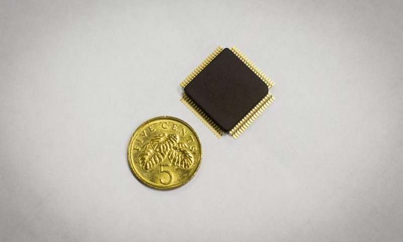
The Verayo technology assigns manufactured chips sets of 128-bit numbers—based on these speed differences—that are stored in a database in the cloud. Integrated into radio frequency identification (RFID) tags, the chips can be scanned by a mobile device or reader that will query the database to determine if the tag is authentic. A different 128-bit number is used for each authentication.
Verayo is currently targeting the consumer-product market, partnering last year with its largest client, Canon Inc., to incorporate Verayo's chips into RFID tags of cameras being sold across China. Other Verayo clients include gift- and loyalty-card providers. The technology can also be used to identify fake licenses and passports.
Now conducting pilot studies with wineries, the company is also seeking to penetrate the consumables market, which could significantly boost sales, Devadas says. "You can build this chip for a nickel, but you have to sell a lot of these chips to make money," he says.
But with more than 40 million chips sold worldwide since 2013, Devadas adds, "This is productization and academic success. As far as I'm concerned, this is great."


Racing signals
PUFs are created during silicon- integrated chip manufacturing, when wires vary in thickness, and the chemical vapor deposition process—used to produce semiconductor wafers—creates microscopic bumps. Depending on these variations, electrons flow with more or less resistance through different paths of the chip, varying processing speeds.
The PUF technology works by "racing" signals across the chips. Two identical electric signals—derived from an input "challenge"—are sent through the chip, at the same time, and assigned two different paths. The signals race toward a latch that measures what signal the chip processed slower or faster—called a "response." The output is a 1 if one path is faster, and 0 if the other is faster. Repeating the process with different input signals for each race will give a 128-bit number—and it can be repeated hundreds of times.
"Then, suddenly, you have a miniscule probability you're going to get the same 128-bit resolution for any given race," Devadas says.
When the tag is scanned, the reader will first identify the tag. Then, it will present the chip with a random challenge of the many that are stored in the database. If the response has 96 or more matching bits, it's considered authentic. Tags are attached to Canon camera packages, which consumers can scan using smartphones with near-field communication.
In 2002, Devadas and other MIT researchers delivered a seminal paper introducing silicon PUF technology at the Computer and Communications Security Conference, which coined the name and described the first integrated PUF circuit. This March, that paper earned an A. Richard Newton Technical Impact Award from the Institute of Electrical and Electronics Engineers and the Association for Computing Machinery—"which is a test of time for the concept and technology," Devadas says.
By 2004, Devadas and his students had developed a few dozen bulky, PUF-enabled circuits, labeling each with a human name, such as "Harold," "Cameron," and "Dennis." They stored the speed characteristics of each in a database on their computer; when a given circuit was scanned using a custom reader, its name would pop up on the screen.
This project earned Devadas a grant from the MIT Deshpande Center for Technological Innovation, and several government grants, which helped Verayo launch in its current Silicon Valley headquarters.

Keeping volatile secrets
Although Verayo is focused on the consumer space, the technology has other uses, such as generating "volatile secret keys," Devadas says, which would only be revealed when activated by voltage.
Because PUF chips do not store such secrets, Devadas says, they need voltage to reveal their unique numeric identification—which could be stored as cryptographic keys. "When the chip powers up, there will be this 128-bit number that gets generated, but it doesn't exist when the chip is powered down," Devadas says. "If I don't have a way of pulling [the key] out, I won't know what it is."
This technology has advantages, Devadas says, over traditional nonvolatile data-storage devices, such as flash or erasable programmable read-only memory chips, which retain hackable data even when switched off. These nonvolatile chips are still difficult to break into, he adds, but not as difficult as PUF-enabled chips, which need to be inspected internally when the chip is powered on and the right challenges are applied.
"All of cryptography is based on something remaining secret," Devadas says. "PUFs are a way of generating those secrets in a more physically secure manner."
Attracting funding from the Department of Defense, this concept could help, for instance, ensure that drones don't connect with hacked servers, or that wearables don't share data with unauthorized servers.
Devadas says the PUF-technology market has seen significant growth in recent years, with other companies now developing in the space. But the competition doesn't discourage the PUF pioneer—in fact, Devadas is excited about the increased interest.
"It does feel like the world is coming around," he says. "And we're still here—that's the beauty of it."


2016年8月15日星期一

What new wearable sensors can reveal you are sweating from perspiration


Wearable sensors measure skin temperature in addition to glucose, lactate, sodium and potassium in sweat. Integrated circuits analyze the data and transmit the information wirelessly to a mobile phone.

When engineers say they are going to make you sweat, it is all in the name of science.

Specifically, it is for a flexible force sensor system that can measure metabolites and electrolytes in sweat, calibrate the data based upon skin temperature and sync the results in real time to a smartphone.
The advance opens doors to wearable devices that alert users to health problems such as fatigue, dehydration and dangerously high body temperatures.
Human sweat contains physiologically rich information, thus making it an attractive body fluid for non-invasive wearable sensors. However, sweat is complex and it is necessary to measure multiple targets to extract meaningful information about your state of health. In this regard, we have developed a fully integrated system that simultaneously and selectively measures multiple sweat analytes, and wirelessly transmits the processed data to a smartphone. Our work presents a technology platform for sweat-based health monitors.
Melody worked with study co-lead authors Wei Gao and Sam Emaminejad, both of whom are postdoctoral fellows in his lab. Emaminejad also has a joint appointment at the Stanford School of Medicine, and all three have affiliations with the Berkeley Sensor and Actuator Center and the Materials Sciences Division at Lawrence Berkeley National Laboratory.
Chemical clues to a person's physical condition
To help design the sweat sensor system, Melody and his team consulted exercise physiologist George Brooks, a UC Berkeley professor of integrative biology. Brooks said he was impressed when Melody  and his team first approached him about the sensor.
"Having a wearable sweat sensor is really incredible because the metabolites and electrolytes measured by the Melody device are vitally important for the health and well-being of an individual," said Brooks, a co-author on the study. "When studying the effects of exercise on human physiology, we typically take blood samples. With this non-invasive technology, someday it may be possible to know what's going on physiologically without needle sticks or attaching little, disposable cups on you."

The prototype developed by Melody and his research team packs five sensors onto a flexible circuit board. The sensors measure the metabolites glucose and lactate, the electrolytes sodium and potassium, and skin temperature.
"The integrated system allows us to use the measured  to calibrate and adjust the readings of other sensors in ," said Gao. "This is important because the response of glucose and lactate sensors can be greatly influenced by temperature."
Developing smart wristbands and headbands
Adjacent to the sensor array is the wireless printed circuit board with off-the-shelf silicon components. The researchers used more than 10 integrated circuit chips responsible for taking the measurements from the sensors, amplifying the signals, adjusting for temperature changes and wirelessly transmitting the data. The researchers developed an app to sync the data from the sensors to mobile phones, and fitted the device onto "smart" wristbands and headbands.
They put the device - and dozens of volunteers - through various indoor and outdoor exercises. Study subjects cycled on stationary bikes or ran outdoors on tracks and trails from a few minutes to more than an hour.
"We can easily shrink this device by integrating all the circuit functionalities into a single chip," said Emaminejad. "The number of biochemicals we target can also be ramped up so we can measure a lot of things at once. That makes large-scale clinical studies possible, which will help us better understand athletic performance and physiological responses to exercise."
Melody noted that a long-term goal would be to use this device for population-level studies for medical applications.
Brooks also noted the potential for the device to be used to measure more than perspiration.
"While Professor Melody's wearable, non-invasive technology works well on sweating athletes, there are likely to be many other applications of the technology for measuring vital metabolite and electrolyte levels of healthy persons in daily life," said Brooks. "It can also be adapted to monitor other body fluids for those suffering from illness and injury."